Every electronic product begins with a physical question: how should its circuits fit, connect, and perform? Circuit board design answers that question through schematic planning, component placement, routing, and manufacturing preparation. It turns electrical intent into a board that can be assembled, tested, repaired, and trusted. A compact medical sensor, industrial controller, or laptop may look different, yet each depends on disciplined layout decisions. Small details matter. A misplaced via can increase noise, weaken thermal performance, or complicate inspection.
Effective circuit board design combines electrical engineering, mechanical awareness, and production experience. Designers consider signal integrity, power distribution, heat flow, component tolerances, and electromagnetic compatibility. They also review spacing, materials, and assembly limits before fabrication. Standards such as IPC guidance can support consistent decisions, but standards do not replace judgment. A simulation may predict clean signals, while a prototype reveals unexpected crosstalk near a fast connector. That is why experienced teams inspect test data, revise layouts, and document each change. Reliable design is evidence-based.
The importance becomes clearest when a board leaves the screen. It must survive vibration, temperature changes, repeated assembly, and everyday user demands. Poor planning can cause costly redesigns, delayed production, or intermittent failures that are difficult to reproduce. No layout is perfect. Trade-offs remain. A smaller board may save space but reduce serviceability. More copper may improve cooling but increase cost and weight. Understanding these tensions helps engineers make defensible choices rather than attractive guesses. This article examines what circuit board design involves, why it shapes product reliability, and how careful methods turn complex requirements into practical hardware.
What Is Circuit Board Design and Why Is It Important?
Definition and Purpose of Circuit Board Design
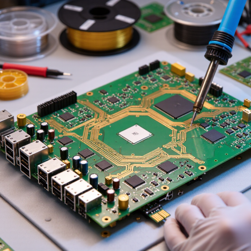
Circuit board design is the process of planning electrical connections, components, and physical layers on a board. Its purpose is practical: convert a circuit idea into a safe, manufacturable, and testable product. Designers create schematics, place components, route traces, and check power distribution. They also manage heat, signal noise, spacing, and mechanical limits. A small routing error can cause unstable voltage or delayed signals. That risk makes design review essential.
Demand for reliable electronics continues to increase. The World Semiconductor Trade Statistics report recorded global semiconductor sales of about 627.6 billion dollars in 2024. It forecast approximately 697 billion dollars for 2025. This growth increases pressure on circuit boards to support higher speeds and smaller layouts. IPC-2221 guidance also emphasizes insulation, current capacity, spacing, and environmental reliability. These details are not decorative. They influence product safety and service life.
Tips: Start with a clear schematic and realistic component footprints. Keep high-current paths short and wide. Separate noisy signals from sensitive circuits. Run design-rule checks before ordering prototypes. Then inspect the physical board carefully. A perfect first revision is unlikely. I still treat unexpected test results as useful evidence, not failure. Record each change, because memory becomes unreliable during fast revisions.
| Data Dimension | Core Data | Design Details and Typical Activities | Why It Matters |
|---|---|---|---|
| Definition | The process of creating the electrical, physical, and manufacturing data needed to produce a printed circuit board assembly. | Circuit board design translates a circuit concept or schematic into a physical board layout containing components, conductive traces, vias, copper areas, and mechanical features. | It connects circuit theory with a manufacturable hardware product. |
| Primary Purpose | To provide reliable electrical connections and mechanical support for electronic components. | The design defines how power, signals, grounds, and components are arranged and interconnected on one or more board layers. | A well-planned board helps the product operate safely, consistently, and according to its technical requirements. |
| Main Design Inputs | Electrical schematic, component requirements, enclosure constraints, operating conditions, and manufacturing rules. | Designers also consider current levels, signal speeds, thermal limits, connector locations, mounting points, component availability, and regulatory requirements. | Complete inputs reduce redesigns caused by electrical, mechanical, or production conflicts. |
| Electrical Layout | Placement and routing of signals, power distribution, and return paths. | The layout establishes trace widths, clearances, layer assignments, impedance-controlled paths, ground planes, decoupling locations, and protection circuits. | Good electrical layout improves signal integrity, power stability, electromagnetic compatibility, and circuit reliability. |
| Layer Structure | A board may use one, two, or multiple copper layers separated by insulating material. | Additional layers can provide dedicated power or ground planes, shorter routing paths, controlled impedance, and improved use of limited board area. | The layer configuration affects performance, manufacturability, thickness, cost, and thermal behavior. |
| Component Placement | The organized physical positioning of electronic components on the board. | Placement commonly follows functional blocks, signal-flow requirements, thermal considerations, connector access, assembly direction, and serviceability needs. | Strategic placement can shorten connections, reduce noise, improve cooling, and simplify assembly and inspection. |
| Signal Integrity | Maintaining the quality and timing of electrical signals as they travel through the board. | Relevant practices include controlled trace geometry, appropriate reference planes, length matching, termination, spacing, and reduction of unwanted reflections and crosstalk. | Signal-integrity control is increasingly important for high-speed digital, radio-frequency, and precision measurement circuits. |
| Power Integrity | Delivering stable voltage and current to every circuit section under expected operating conditions. | Design work may include power-plane planning, voltage-drop analysis, decoupling capacitors, current-capacity checks, thermal assessment, and separation of sensitive and noisy domains. | Stable power reduces resets, interference, timing problems, overheating, and premature component stress. |
| Thermal Management | Controlling heat generated by components and conductive paths. | Designers may use copper areas, thermal vias, heat-spreading structures, component spacing, airflow paths, and heat sinks where necessary. | Keeping temperatures within component limits supports performance, safety, and long service life. |
| Design Verification | Checking that the layout satisfies the schematic, design rules, and product requirements. | Verification can include electrical rule checks, design rule checks, netlist comparison, clearance analysis, current-capacity review, manufacturability checks, and simulation. | Early verification identifies errors before fabrication, reducing material waste, delays, and costly physical rework. |
| Manufacturing Documentation | A set of digital files and drawings used to fabricate and assemble the board. | Typical documentation includes fabrication data, assembly placement data, solder-paste data, a bill of materials, drill information, board drawings, and revision details. | Accurate documentation ensures that production interprets the design consistently and traceably. |
| Design for Manufacturing | Adapting the design to the capabilities and limits of board fabrication and assembly processes. | Considerations include trace and spacing limits, hole sizes, pad geometry, component spacing, solder access, panelization, inspection, and testing. | Manufacturing-aware design improves yield, reduces production defects, and helps control unit cost. |
| Reliability Factors | The board’s ability to perform consistently throughout its expected operating life. | Reliability depends on material selection, electrical margins, thermal cycling, vibration resistance, moisture protection, connector design, solder-joint quality, and testing. | Reliable circuit boards reduce field failures, maintenance requirements, safety risks, and total ownership cost. |
| Final Outcome | A verified and manufacturable board design ready for prototype fabrication and production release. | The completed design should meet functional, mechanical, thermal, electrical, regulatory, cost, and production requirements. | A disciplined design process helps transform an electronic concept into a practical, repeatable, and scalable product. |