How to Design Advanced PCB for High Performance Electronics?
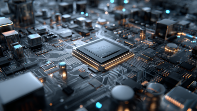
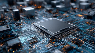
In the realm of high-performance electronics, the design of advanced PCB is crucial. It serves as the foundation for effective connectivity and functionality of various components. A well-designed advanced PCB can enhance signal integrity, reduce noise, and improve thermal management. These factors are essential for achieving optimal performance in demanding applications.
Engineers face numerous challenges when designing advanced PCBs. Choosing the right materials, layer counts, and routing techniques is not straightforward. Each decision can significantly impact performance. For instance, a wrong trace width can lead to inadequate current handling. Designers must balance performance with cost constraints, which can complicate their objectives.
Moreover, testing and validation of advanced PCBs can be intricate. Simulation tools can help predict potential issues, but they are not foolproof. Iterative design processes often uncover flaws that require reworking. These experiences highlight the need for continuous learning and adaptation in the design journey of advanced PCB. This ongoing reflection is vital for pushing the boundaries of what's possible in high-performance electronics.

Understanding the Basics of High Performance Electronics in PCB Design
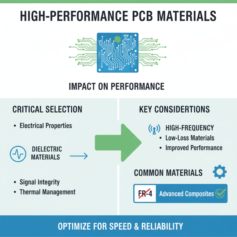
When designing high-performance electronics, understanding the basics of PCB design is crucial. High-speed signals and power delivery must be carefully considered. These factors can affect overall device reliability and performance. Avoiding signal interference and managing heat dissipation are vital to a successful design. Materials used also play a role. Choosing the right substrate can enhance signal integrity.
Tips: Always prioritize grounding techniques. A proper ground plane helps reduce electromagnetic interference. Consider using multiple layers for complex circuits. Each layer can serve a specific purpose, alleviating signal crosstalk. However, be cautious with layer count. More layers may complicate the design process.
It's essential to think about component placement. Crowded layouts can lead to increased heat and reduced reliability. Spacing components out, while balancing traces, is an art in itself. Often, the most straightforward designs outperform complicated ones. Reflect on your layout choices regularly. Make adjustments as necessary for optimal results.
Key Design Principles for Advanced PCB Layouts
Designing advanced PCBs requires a deep understanding of key principles. Effective layout is critical for high-performance electronics. In fact, up to 70% of electronic failures can be traced back to PCB design flaws. Engineers must prioritize signal integrity, grounding, and power distribution in their designs. This attention to detail directly impacts performance and reliability.
Signal integrity hinges on proper routing techniques. Keep traces as short as possible. This reduces inductance and enhances performance. Differential pairs should be coupled and routed together. The impedance control is essential; deviations can lead to over 10% signal degradation. Ground planes should be continuous, minimizing loop areas to reduce electromagnetic interference.
Power distribution networks (PDNs) require careful planning. Analyze current paths and ensure adequate voltage levels. Using decoupling capacitors effectively can smoothen transient demands. Yet, it’s common to underestimate power integrity issues. Many engineers face challenges in balancing the needs of High-Frequency designs with thermal management. Striking this balance often leads to iterative design processes needing further refinement. Keep testing different configurations—it's an unavoidable part of PCB design.
Techniques for Thermal Management in Advanced PCB Design
Thermal management is critical in advanced PCB design. High-performance electronics generate significant heat. If not managed well, this can lead to failure. Designers face challenges in ensuring temperature control. They must consider materials, layout, and component placement.
Using thermal vias is one effective technique. These allow heat to transfer from components to heat sinks. Adequate spacing between high-power parts is essential as well. It can prevent heat buildup. However, many forget to calculate the thermal impedance accurately. This is a common oversight.
Properly designed airflow can also enhance cooling efficiency. Ventilation paths should be considered early in the design. Yet, many designers neglect this detail. They focus too much on aesthetics or functionality. Balancing performance and heat dissipation requires careful thought. Revisiting designs to optimize thermal paths is often necessary. It’s an ongoing learning process.
Best Practices for Signal Integrity and Electromagnetic Compatibility
When designing advanced PCBs for high-performance electronics, signal integrity and electromagnetic compatibility (EMC) are crucial. Designers often face challenges with noise and interference. A common mistake is neglecting ground planes. They are essential for reducing electromagnetic interference. A poor ground plane can lead to significant signal degradation.
Another aspect to consider is trace width. Wider traces reduce resistance but may cause issues with impedance. Balancing these factors can be tricky. Designers sometimes overlook the effects of via placement. Improper via location can create inductance issues, leading to signal distortion. Every detail counts in high-speed designs.
Effective shielding techniques can enhance EMC. Placing components thoughtfully can mitigate emissions. However, these strategies do not guarantee perfection. Sometimes, unexpected interference arises. Continuous testing is necessary. A well-designed PCB may still require tweaks. It's crucial to remain vigilant and adaptable throughout the design process.