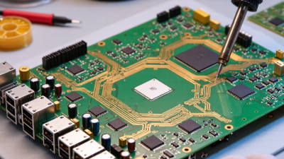
Choosing among the top PCB layout services for global buyers requires more than comparing prices. It requires evidence, engineering judgment, and clear communication across borders. A reliable provider should show completed projects, revision records, design-rule checks, and measurable results. Look for experience with multilayer boards, high-speed signals, thermal constraints, controlled impedance, and manufacturability. Small details matter. A misplaced via can disrupt signal integrity. An undersized copper path can create unwanted heat.
Henry W. Ott, a respected EMC engineer and author, stated, “The best way to control EMI is at the source.” His principle remains highly relevant to modern pcb layout. Skilled teams reduce electromagnetic problems during placement and routing, rather than correcting them after fabrication. They study return paths, separate noisy circuits, shorten critical traces, and protect sensitive interfaces. Practical proof matters more than attractive promises.
Global buyers should also examine workflow discipline. Can the provider work with Altium, KiCad, OrCAD, or Eagle files? Are component libraries verified? Are fabrication outputs reviewed by an experienced engineer? Can the team explain decisions in clear English? These questions expose weak processes quickly.
No provider is perfect. Even experienced engineers can miss a constraint when requirements change late. That is why review checkpoints, documented assumptions, and independent checks remain essential. A strong service does not simply deliver files. It helps create a board that can be assembled, tested, repaired, and scaled with confidence. The best choice balances technical depth, transparent communication, and demonstrated reliability.
PCB layout services turn an electrical schematic into a manufacturable board design. A layout engineer places components, routes traces, and defines layer construction. The work connects circuit intent with physical production limits. It also considers signal speed, heat, noise, safety, and assembly access. In global projects, clear documentation reduces misunderstandings between designers, fabricators, and assemblers.
The scope may include stack-up planning, component placement, fanout, routing, and design-rule setup. Engineers review impedance targets for high-speed nets and isolate sensitive analog paths. They check copper balance, return paths, creepage, clearances, and thermal reliefs. Practical review matters. A board can pass software checks yet fail during soldering or testing. That gap is easy to underestimate.
Core deliverables normally include native layout files, fabrication drawings, assembly drawings, drill data, and a bill of materials. A reliable package also includes production outputs, revision notes, and a completed design-rule report. For controlled designs, impedance tables and test-point information should remain traceable to the schematic. Experienced teams request manufacturing feedback before release, not after a rejected panel. I have found that late component substitutions often expose weak footprint libraries. That is an imperfect part of the process, but it deserves review.
Choosing a PCB layout service requires more than comparing hourly rates. In practical reviews, assess schematic interpretation, stackup planning, impedance control, and design-for-manufacturing discipline. Ask for anonymized examples showing dense BGA fanout, thermal vias, and controlled-length differential pairs. The provider should explain decisions clearly, not merely deliver files.
Industry data adds useful context. IPC’s June 2024 North American PCB Statistical Program reported a 1.10 book-to-bill ratio, indicating continued production planning pressure. That pressure makes revision control and delivery capacity important evaluation criteria. Confirm whether the team uses IPC-2221 and IPC-7351 guidance, performs automated rule checks, and completes an independent design review. Request measurable details, such as average review cycles, defect escape rates, and response times.
Communication needs testing. Send a small technical question before signing. Notice the reply speed and precision. A capable provider should identify missing fabrication notes, unclear tolerances, and risky component spacing early. Security also matters; ask about access controls, encrypted file transfer, and documented retention policies. References can help, but they are not perfect evidence. A provider may present only successful projects. A trial layout, with agreed acceptance criteria, reveals more than polished claims. Cost still matters, yet an unusually low quote may hide weak checking, rushed routing, or expensive rework. Personally, I would score technical depth above presentation quality, while admitting that scorecards can overlook team chemistry and late-stage engineering judgment.
| Comparison Criterion | What to Compare | Strong Service-Provider Indicators | Typical Evidence or Deliverables | Questions for Global Buyers |
|---|---|---|---|---|
| Engineering Scope | Schematic capture, component placement, routing, library creation, design-rule setup, and documentation support. | A clearly defined scope with responsibilities separated between the buyer and the layout team. | Statement of work, milestone plan, engineering assumptions, and revision-control procedure. | Does the quotation include schematic review, footprint creation, placement review, and final manufacturing files? |
| Board Complexity | Layer count, component density, high-speed interfaces, fine-pitch packages, rigid-flex requirements, and controlled-impedance nets. | Documented experience with multilayer, high-density interconnect, mixed-signal, RF, or rigid-flex designs relevant to the project. | Redacted sample layouts, capability matrix, stack-up examples, and engineering review records. | Can the provider support the required package types, via structures, trace geometries, and board materials? |
| CAD Tool Compatibility | Native design-tool support and the ability to exchange data without losing constraints, net classes, libraries, or design intent. | Use of the buyer’s required CAD platform or a controlled workflow for importing and exporting neutral data. | Native CAD files, approved library files, netlists, constraints, and version information. | Which software versions are supported, and who owns the native source files after project completion? |
| Design-for-Manufacturing Review | Checks for fabrication, assembly, test access, solderability, component spacing, drill limitations, copper balance, and panelization. | DFM and DFA checks are performed before release rather than only after a manufacturer identifies a problem. | DFM/DFA checklist, flagged-issue log, manufacturability report, and corrective-action history. | Are fabrication and assembly rules supplied by the selected manufacturer included in the layout review? |
| Signal Integrity | Controlled impedance, length matching, differential-pair routing, return paths, crosstalk risk, and power-integrity considerations. | High-speed constraints are documented and verified against the stack-up and interface requirements. | Impedance table, length-matching report, differential-pair rules, return-path review, and simulation results when required. | Which interfaces require controlled impedance or timing matching, and who supplies the electrical constraints? |
| Layer Stack-Up Development | Layer count, dielectric thickness, copper weights, material selection, impedance targets, and power/ground distribution. | The stack-up is agreed with the fabricator or based on verified fabrication capabilities before routing begins. | Approved stack-up drawing, material specification, impedance calculations, and fabricator feedback. | Is the stack-up preliminary or fabrication-approved, and can it be adjusted for regional material availability? |
| Standards and Rule Control | Use of recognized PCB design and documentation practices, including relevant IPC guidance and customer-specific rules. | Applicable requirements are recorded in a project rule set instead of being treated as informal assumptions. | Design-rule file, constraint table, fabrication notes, assembly notes, and revision-controlled specifications. | Which IPC or customer standards apply, and how are exceptions documented and approved? |
| Output Data Package | Completeness and consistency of manufacturing, assembly, testing, and source-design files. | The release package is checked for consistency across Gerber or ODB++ data, drill files, drawings, BOM, pick-and-place data, and source files. | Gerber ODB++ NC Drill BOM Pick-and-Place Fabrication Drawing Assembly Drawing | Is a pre-release checklist used, and are all output files generated from the same approved revision? |
| Review and Verification | Electrical-rule checking, design-rule checking, 3D clearance review, peer review, and release approval. | At least one independent review is completed before the design is released for fabrication. | DRC/ERC reports, 3D review images, peer-review checklist, issue tracker, and sign-off record. | Who performs the independent review, and are unresolved warnings clearly listed in the release documentation? |
| Typical Turnaround Planning | Schedule for initial placement, routing, review cycles, and final data release. | The schedule is based on board complexity, input readiness, component-library status, and the number of expected review cycles. | Milestone schedule, assumptions, response-time commitments, and revision limits. | What is the estimated working time for the first layout, each review cycle, and the final release? |
| Revision Management | Handling of engineering-change orders, component substitutions, layout updates, and release history. | Every change is traceable to a revision, request, approval, and updated output package. | Revision log, ECO process, file-naming convention, change summary, and archived release packages. | How are late component changes handled, and what is included in the quoted revision allowance? |
| Component Library Quality | Accuracy of symbols, footprints, 3D models, courtyard definitions, polarity marks, thermal pads, and land patterns. | Footprints are checked against manufacturer datasheets and approved before placement and routing. | Library approval sheet, datasheet references, footprint review images, and 3D component models where available. | Does the provider create missing footprints, and who approves them before they enter the production design? |
| Manufacturing and Assembly Network | Ability to coordinate with fabricators and assemblers in different regions without making unsupported claims about capacity. | The provider can work with the buyer’s nominated suppliers and adapt the design to their documented capabilities. | Supplier capability files, fabrication feedback, assembly constraints, and approved manufacturing notes. | Can the layout be optimized for multiple approved suppliers or a specific regional manufacturing process? |
| Communication Across Time Zones | Meeting availability, response times, technical English, documentation quality, and escalation procedures. | A named technical contact, written action items, and an agreed communication window are provided. | Communication plan, meeting schedule, issue tracker, response-time policy, and escalation matrix. | How will urgent design questions be handled when the buyer and engineering team work in different time zones? |
| Data Security and Confidentiality | Protection of schematics, source files, component data, customer information, and intellectual property. | Confidentiality terms, access control, secure file transfer, backup policy, and employee access procedures are documented. | NDA, information-security policy, access permissions, secure portal details, and data-retention terms. | Where are project files stored, who can access them, and how are files deleted or returned after completion? |
| Pricing Transparency | Fixed project fee, hourly engineering rate, milestone billing, revision charges, and optional analysis costs. | The quotation identifies assumptions, inclusions, exclusions, review cycles, and change-order rates. | Itemized quotation, payment milestones, revision policy, travel or meeting charges, and tax or currency terms. | Are library creation, stack-up work, impedance analysis, DFM iterations, and urgent changes priced separately? |
| Post-Release Support | Support during prototype fabrication, assembly, testing, field changes, and transition to production. | Defined support coverage is available after release, with clear limits for included engineering assistance. | Support terms, prototype-feedback process, failure-analysis workflow, and production handoff checklist. | How are fabrication queries, assembly defects, and engineering changes handled after the initial release? |
| Overall Selection Method | Balance of technical capability, process control, communication, security, schedule, and total project cost. | The buyer evaluates documented evidence rather than choosing solely on hourly price or promised turnaround. | Weighted supplier scorecard, sample deliverable review, technical interview, and pilot-project results. | Does the provider meet the project’s mandatory requirements, and can its process scale to future revisions or product variants? |

A reliable PCB layout begins before any trace is routed. Engineers review schematic files, board outlines, layer requirements, component libraries, and manufacturing notes. They check net names against the bill of materials and confirm critical interfaces. Missing data is common. A footprint may look correct but still use the wrong courtyard. That small error can move a connector by several millimeters. Experienced teams record open questions instead of silently guessing. They also define impedance targets, current paths, thermal zones, and assembly limits before placement starts.
During placement, high-speed parts stay close to their supporting components. Decoupling capacitors sit beside power pins, with short, wide connections. Sensitive analog sections remain separated from noisy switching nodes. The layout then moves through power, ground, signal, and fanout routing. Designers inspect return paths, via transitions, copper spacing, and heat flow. Automated checks help, but they do not replace engineering judgment. A clean report can still hide a weak reference plane. This is where practical review matters.
Before release, the team runs design-rule checks, electrical-rule checks, and manufacturability reviews. They compare fabrication plot files with the source layout. Drill tables, stackup data, assembly drawings, placement files, and the revised bill of materials must agree. A second engineer reviews critical nets and polarity marks. Sometimes the first export fails. That is useful evidence, not embarrassment. The files are corrected, regenerated, and checked again. Final outputs should be traceable, readable, and ready for fabrication without guesswork.
Technical standards should guide every layout decision, not decorate a compliance file. Experienced engineers check stack-up design, controlled impedance, creepage, clearance, and thermal paths before routing begins. They also review drill tolerances, copper thickness, and solder mask alignment against the buyer’s manufacturing limits. Details matter. A clean layout reduces rework and protects signal performance.
Quality control must continue beyond automated design-rule checks. Skilled teams compare Gerber files with fabrication drawings, inspect first-article boards, and verify dimensions through documented measurements. Electrical testing should cover continuity, isolation, and critical net performance. Records must match. Traceability for materials, revisions, inspections, and corrective actions gives global buyers stronger control across suppliers.
Regulatory compliance requires practical evidence. A reliable service provider can support declarations for restricted substances, material composition, fire performance, and product safety requirements. Documentation should remain current for the destination market. I have seen projects delayed because a correct board lacked a correct certificate. That mistake is avoidable, but not always avoided. Engineers should question unclear requirements, confirm regional rules, and preserve approval records. A perfect first-pass layout is rare. Careful review still makes it more likely.
Top PCB Layout Services for Global Buyers
Selecting a PCB layout partner for international projects requires more than attractive pricing. Grand View Research valued the global PCB market at approximately US$89 billion in 2023. That scale increases pressure on design accuracy, production readiness, and cross-border communication. A capable partner should understand IPC design standards, controlled impedance, thermal relief, creepage distances, and high-density routing. Ask for documented experience with your board type, layer count, material stack-up, and target factory process.
International work also depends on practical coordination. The partner should provide clear English documentation, revision control, timezone coverage, and secure file handling. Request native CAD files, fabrication drawings, assembly notes, Gerbers, drill files, and a design-for-manufacturing report. IPC’s 2024 International Technology Roadmap for Electronic Interconnections highlights miniaturization, high-speed signaling, and manufacturing resilience as continuing industry priorities. Your layout team should reflect those realities, not merely complete connections.
Small details expose real capability. Check whether the designer flags an unbalanced stack-up, an inaccessible test point, or a connector placed two millimeters too close to the enclosure wall. I have seen projects delayed because a “finished” layout ignored regional component availability. A perfect first review may even be suspicious. Good partners explain trade-offs, record assumptions, and invite correction. Their process should include independent checks for signal integrity, power distribution, manufacturability, and compliance before release. Some recommendations may still need revision after prototype testing. That is normal, and honest teams say so.
A 100-point evaluation framework for selecting a PCB layout partner for international project requirements. Higher scores indicate greater procurement priority.
Documentation quality, DFM capability, signal integrity, international communication, and revision control are key factors in reducing design risk across global PCB projects.
| Cookie | Duration | Description |
|---|---|---|
| cookielawinfo-checkbox-analytics | 11 months | This cookie is set by GDPR Cookie Consent plugin. The cookie is used to store the user consent for the cookies in the category "Analytics". |
| cookielawinfo-checkbox-functional | 11 months | The cookie is set by GDPR cookie consent to record the user consent for the cookies in the category "Functional". |
| cookielawinfo-checkbox-necessary | 11 months | This cookie is set by GDPR Cookie Consent plugin. The cookies is used to store the user consent for the cookies in the category "Necessary". |
| cookielawinfo-checkbox-others | 11 months | This cookie is set by GDPR Cookie Consent plugin. The cookie is used to store the user consent for the cookies in the category "Other. |
| cookielawinfo-checkbox-performance | 11 months | This cookie is set by GDPR Cookie Consent plugin. The cookie is used to store the user consent for the cookies in the category "Performance". |
| viewed_cookie_policy | 11 months | The cookie is set by the GDPR Cookie Consent plugin and is used to store whether or not user has consented to the use of cookies. It does not store any personal data. |